Atari Tetris |
Post Reply 
|
| Author | |
anks 
Level Up 

Joined: 13 October 2007 Status: Offline Points: 99 |
 Post Options Post Options
") Thanks(1) Thanks(1)
 Quote Reply Quote Reply
 Topic: Atari Tetris Topic: Atari TetrisPosted: 24 August 2010 at 7:45pm |
|
Atari Tetris Repair log The board itself looks in quite good nick so I decided to rescue it from the scrap parts pile. 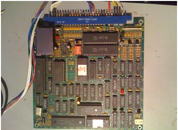 Symptom garbage on screen 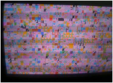 After a quick inspection of the board all I noticed was a track that needed patching up but that made no difference to the problem. I then decided that a quick check of the rom’s was a good way forward but they came back as perfect matches to the mame rom set. I had a quick look and noticed that the ram located at F30 (video ram Part No. V61C16S55L) and the ram at B40 (programe ram Part No. HY6264-P15) were in sockets. The video ram had obviously been pulled before and someone had used a wide socket cut up to make a slim. I removed the ram to check in my programmer but both came back fine. I hen checked the soldering on the socket and all seemed to be fine as well even if it was messy (I’m not calling too much Atari boards I fine are a paint to de-solder and solder). At this point I decided that it was time to break out the scope and find out what was going on with the 6502 CPU. Inspection on the clock line showed it to be healthy (see pic) but the addresses lines were showing no activity that pointed me to the reset line. 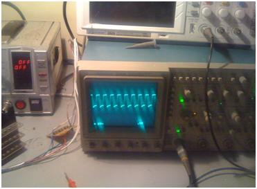 The reset line was being held low but me having very little knowledge of the 6502 made me go dig for the datasheet and from what I could understand (correct me if I’m wrong) that the line should be held low for at least two clock cycles on power up then held high once the voltage has reached over 4.75 volts. So I decided to force the reset pin high with a probe connected to 5 volts on the jamma harness and the game jumped into life. 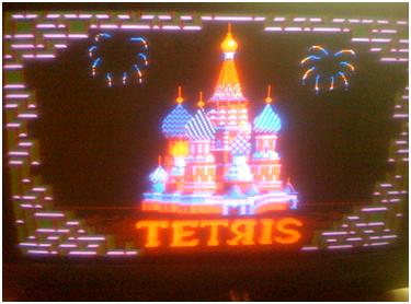 Well so now I knew there was a problem with the reset or watchdog circuit preventing the cpu from initialising. I traced the reset line to pin 1(1CLR) on 2 SN74LS74AN and also pin 13 (2CLR) on the second after it also goes to pin 12 on a SN74LS197N (output Qd). The connections to the two LS74 were inputs so were more than likely to connect other parts of the circuit to reset (don’t hold me to that) so the LS192 must be responsible for the power on reset. I’ve seen this before with other Atari hardware from around the same era and remember that in the system1 schematics Id seen a similar circuit used. So after a quick look I decided to look at the input on pin13 that is driven by a transistor at B10. This looked ok and all the solder looked fine but with a little pressure I noticed that the leg had become snapped but was still lined up so looked fine. With a little solder the problem with the reset was fixed. I should of checked this better in the first place has there is now a red LED that is illuminated next to the area the transistor is located not that this is always a cause for concern as I’ve seen loads of PCB’s that have LED’s that seem only to be there for decoration.
New symptom now it seems the game reports a bad video ram probably why it had been pulled at some stage. Even with the video ram error the game seemed to have all the right colours and looked fine. I placed some pressure on the area the ram was located and fired the board up straight into test and found that the video ram problem had gone. Recycled the process without the pressure and the video ram fault was back. Well remember about the messy soldering I said was fine. A little touching up and the board fired up and worked fine. Well I made that job harder than it had to be. I was hoping to get some better pic’s of the board but my Iphone camera is not really up to the task. Ive no idea how ive made it look like this but if moderator can sort it cause I cant work it out Cheers Kris Edit: To remove bad text links Edited by Aran - 10 September 2010 at 1:26pm |
|
 |
|
|
mastercello
Bonus Stage 

Joined: 18 August 2009 Location: Switzerland Status: Offline Points: 259 |
Post Options
Thanks(0)
Quote Reply
Posted: 13 June 2014 at 3:28pm |
|
I got a defective Tetris PCB from a friend for repair.
It has the same problem like the one above from anks. Anyone has a schematic for this Atari Tetris pcb? Not easy to find the problem at this watchdog circuit for me, where to start? Just exchange the 74LS197 to start with? Appreciate any help...cheers!
|
|
|
|
|
mastercello
Bonus Stage
Joined: 18 August 2009 Location: Switzerland Status: Offline Points: 259 |
Post Options
Thanks(0)
Quote Reply
Posted: 18 June 2014 at 7:18am |
|
Anyone please!

|
|
|
|
|
Post Reply
|
|
 Tweet
Tweet
|
| Forum Jump | Forum Permissions You cannot post new topics in this forum You cannot reply to topics in this forum You cannot delete your posts in this forum You cannot edit your posts in this forum You cannot create polls in this forum You cannot vote in polls in this forum |


 Topic Options